- 您现在的位置:买卖IC网 > Sheet目录3861 > PIC18F45K80-I/ML (Microchip Technology)MCU PIC 32KB FLASH 44QFN
PIC18F66K80 FAMILY
DS39977F-page 176
2010-2012 Microchip Technology Inc.
TABLE 11-2:
SUMMARY OF REGISTERS ASSOCIATED WITH PORTA
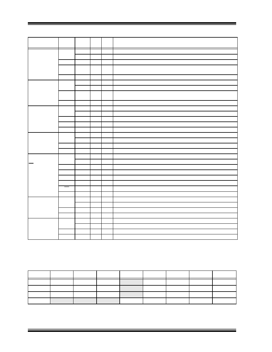
TABLE 11-1:
PORTA FUNCTIONS
Pin Name
Function
TRIS
Setting
I/O
Type
Description
RA0/CVREF/AN0/
ULPWU
RA0
0
O
DIG LATA<0> data output; not affected by analog input.
1
I
ST
PORTA<0> data input; disabled when analog input is enabled.
CVREF
x
O
ANA Comparator voltage reference output. Enabling this feature disables digital I/O.
AN0
1
I
ANA A/D Input Channel 0. Default input configuration on POR; does not affect
digital output.
ULPWU
1
O
DIG Ultra Low-Power Wake-up input.
RA1/AN1/C1INC
RA1
0
O
DIG LATA<1> data output; not affected by analog input.
1
I
ST
PORTA<1> data input; disabled when analog input is enabled.
AN1
1
I
ANA A/D Input Channel 1. Default input configuration on POR; does not affect
digital output.
C1INC(1)
x
I
ANA Comparator 1 Input C.
RA2/VREF-/AN2/
C2INC
RA2
0
O
DIG LATA<2> data output; not affected by analog input.
1
I
ST
PORTA<2> data input; disabled when analog functions are enabled.
VREF-
1
I
ANA A/D and comparator low reference voltage input.
AN2
1
I
ANA A/D Input Channel 2. Default input configuration on POR.
C2INC(1)
x
I
ANA Comparator 2 Input C.
RA3/VREF+/AN3
RA3
0
O
DIG LATA<3> data output; not affected by analog input.
1
I
ST
PORTA<3> data input; disabled when analog input is enabled.
VREF+
1
I
ANA A/D Input Channel 3. Default input configuration on POR.
AN3
1
I
ANA A/D and comparator high reference voltage input.
RA5/AN4/C2INB/
HLVDIN/T1CKI/
SS/CTMUI
RA5
0
O
DIG LATA<5> data output; not affected by analog input.
1
I
ST
PORTA<5> data input; disabled when analog input is enabled.
AN4
1
I
ANA A/D Input Channel 4. Default configuration on POR.
C2INB(2)
1
I
ANA Comparator 2 Input B.
HLVDIN
1
I
ANA High/Low-Voltage Detect external trip point input.
T1CKI
x
I
ST
Timer1 clock input.
SS
1
I
ST
Slave select input for MSSP module.
CTMUI(2)
x
O
—
CTMU pulse generator charger for the C2INB comparator input.
RA6/OSC2/
CLKOUT
RA6
0
O
DIG LATA<6> data output; disabled when FOSC2 Configuration bit is set.
1
I
ST
PORTA<6> data input; disabled when FOSC2 Configuration bit is set.
OSC2
x
O
ANA Main oscillator feedback output connection (HS, XT and LP modes).
CLKOUT
x
O
DIG System cycle clock output (FOSC/4) (EC and INTOSC modes).
RA7/OSC1/CLKIN
RA7
0
O
DIG LATA<7> data output; disabled when FOSC2 Configuration bit is set.
1
I
ST
PORTA<7> data input; disabled when FOSC2 Configuration bit is set.
OSC1
x
I
ANA Main oscillator input connection (HS, XT, and LP modes).
CLKIN
x
I
ANA Main external clock source input (EC modes).
Legend:
O = Output; I = Input; ANA = Analog Signal; DIG = CMOS Output; ST = Schmitt Trigger Buffer Input;
x
= Don’t care (TRIS bit does not affect port direction or is overridden for this option)
Note
1:
This pin assignment is unavailable for 28-pin devices (PIC18F2XK80).
2:
This pin assignment is only available for 28-pin devices (PIC18F2XK80).
Name
Bit 7
Bit 6
Bit 5
Bit 4
Bit 3
Bit 2
Bit 1
Bit 0
PORTA
RA7(1)
RA6(1)
RA5
—
RA3
RA2
RA1
RA0
LATA
LATA7(1)
LATA6(1)
LATA5
—
LATA3
LATA2
LATA1
LATA0
TRISA
TRISA7(1)
TRISA6(1)
TRISA5
—
TRISA3
TRISA2
TRISA1
TRISA0
ANCON0
ANSEL7
ANSEL6
ANSEL5
ANSEL4
ANSEL3
ANSEL2
ANSEL1
ANSEL0
Legend:
— = unimplemented, read as ‘0’. Shaded cells are not used by PORTA.
Note 1:
These bits are enabled depending on the oscillator mode selected. When not enabled as PORTA pins,
they are disabled and read as ‘x’.
发布紧急采购,3分钟左右您将得到回复。
相关PDF资料
PIC24F32KA302-I/ML
MCU 32KB FLASH 2KB RAM 28-QFN
PIC18LF45K80-I/ML
MCU PIC ECAN 32KBFLASH 44QFN
PIC18F4221-I/PT
IC PIC MCU FLASH 2KX16 44TQFP
PIC18F1320-I/SO
IC MCU FLASH 4KX16 A/D 18SOIC
PIC18LF2321-I/SS
IC PIC MCU FLASH 4KX16 28SSOP
PIC16F917-I/PT
IC PIC MCU FLASH 8KX14 44TQFP
PIC18F1320-I/SS
IC MCU FLASH 4KX16 A/D 20SSOP
PIC24FV32KA301-I/P
MCU 32KB FLASH 2KB RAM 20-PDIP
相关代理商/技术参数
PIC18F45K80-I/P
功能描述:8位微控制器 -MCU 32KB FL 4KBRM 16MIPS 12bit ADC CTMU RoHS:否 制造商:Silicon Labs 核心:8051 处理器系列:C8051F39x 数据总线宽度:8 bit 最大时钟频率:50 MHz 程序存储器大小:16 KB 数据 RAM 大小:1 KB 片上 ADC:Yes 工作电源电压:1.8 V to 3.6 V 工作温度范围:- 40 C to + 105 C 封装 / 箱体:QFN-20 安装风格:SMD/SMT
PIC18F45K80-I/PT
功能描述:8位微控制器 -MCU 32KB FL 4KBRM 16MIPS 12bit ADC CTMU RoHS:否 制造商:Silicon Labs 核心:8051 处理器系列:C8051F39x 数据总线宽度:8 bit 最大时钟频率:50 MHz 程序存储器大小:16 KB 数据 RAM 大小:1 KB 片上 ADC:Yes 工作电源电压:1.8 V to 3.6 V 工作温度范围:- 40 C to + 105 C 封装 / 箱体:QFN-20 安装风格:SMD/SMT
PIC18F45K80T-I/ML
功能描述:8位微控制器 -MCU 32KB FL 4KBRM 16MIPS 12bit ADC CTMU RoHS:否 制造商:Silicon Labs 核心:8051 处理器系列:C8051F39x 数据总线宽度:8 bit 最大时钟频率:50 MHz 程序存储器大小:16 KB 数据 RAM 大小:1 KB 片上 ADC:Yes 工作电源电压:1.8 V to 3.6 V 工作温度范围:- 40 C to + 105 C 封装 / 箱体:QFN-20 安装风格:SMD/SMT
PIC18F45K80T-I/PT
功能描述:8位微控制器 -MCU 32KB FL 4KBRM 16MIPS 12bit ADC CTMU RoHS:否 制造商:Silicon Labs 核心:8051 处理器系列:C8051F39x 数据总线宽度:8 bit 最大时钟频率:50 MHz 程序存储器大小:16 KB 数据 RAM 大小:1 KB 片上 ADC:Yes 工作电源电压:1.8 V to 3.6 V 工作温度范围:- 40 C to + 105 C 封装 / 箱体:QFN-20 安装风格:SMD/SMT
PIC18F4610-E/ML
功能描述:8位微控制器 -MCU 64KB 3968 RAM 36 I/O RoHS:否 制造商:Silicon Labs 核心:8051 处理器系列:C8051F39x 数据总线宽度:8 bit 最大时钟频率:50 MHz 程序存储器大小:16 KB 数据 RAM 大小:1 KB 片上 ADC:Yes 工作电源电压:1.8 V to 3.6 V 工作温度范围:- 40 C to + 105 C 封装 / 箱体:QFN-20 安装风格:SMD/SMT
PIC18F4610-E/P
功能描述:8位微控制器 -MCU 64KB 3968 RAM 36 I/O RoHS:否 制造商:Silicon Labs 核心:8051 处理器系列:C8051F39x 数据总线宽度:8 bit 最大时钟频率:50 MHz 程序存储器大小:16 KB 数据 RAM 大小:1 KB 片上 ADC:Yes 工作电源电压:1.8 V to 3.6 V 工作温度范围:- 40 C to + 105 C 封装 / 箱体:QFN-20 安装风格:SMD/SMT
PIC18F4610-E/PT
功能描述:8位微控制器 -MCU 64KB 3968 RAM 36 I/O RoHS:否 制造商:Silicon Labs 核心:8051 处理器系列:C8051F39x 数据总线宽度:8 bit 最大时钟频率:50 MHz 程序存储器大小:16 KB 数据 RAM 大小:1 KB 片上 ADC:Yes 工作电源电压:1.8 V to 3.6 V 工作温度范围:- 40 C to + 105 C 封装 / 箱体:QFN-20 安装风格:SMD/SMT
PIC18F4610-I/ML
功能描述:8位微控制器 -MCU 64KB 3968 RAM 36 I/O RoHS:否 制造商:Silicon Labs 核心:8051 处理器系列:C8051F39x 数据总线宽度:8 bit 最大时钟频率:50 MHz 程序存储器大小:16 KB 数据 RAM 大小:1 KB 片上 ADC:Yes 工作电源电压:1.8 V to 3.6 V 工作温度范围:- 40 C to + 105 C 封装 / 箱体:QFN-20 安装风格:SMD/SMT